- 您现在的位置:买卖IC网 > Sheet目录1223 > KIT33880DWBEVB (Freescale Semiconductor)KIT EVAL FOR MC33880 8X SW W/SPI
�� �
�
�FUNCTIONAL� DEVICE� OPERATION�
�OPERATIONAL� MODES�
�SHORTED� LOAD� FAULT�
�A� shorted� load� (overcurrent)� fault� can� be� caused� by� any�
�output� being� shorted� directly� to� supply� or� an� output� causing�
�the� device� to� current� limit� (linear� short).�
�There� are� two� safety� circuits� progressively� in� operation�
�during� load� short� conditions� providing� system� protection:�
�1.� The� device’s� output� current� is� monitored� in� an� analog�
�fashion� using� SENSEFET� ?� approach� and� current�
�Drain-to-Source� Clamp�
�Voltage� (V� CL� =� 45� V)�
�Drain� Current�
�(I� D� =� 0.3� A)�
�Drain� Voltage�
�Clamp� Energy�
�(E� J� =� I� A� x� V� CL� )�
�limited.�
�2.� The� device’s� output� thermal� limit� is� sensed� and� when�
�attained� causes� only� the� specific� faulted� output� to� shut�
�down.� The� output� will� remain� off� until� cooled.� The�
�device� will� then� reassert� the� output� automatically.� The�
�cycle� will� continue� until� the� fault� is� remove� or� the�
�command� bit� instructs� the� output� off.�
�UNDERVOLTAGE� SHUTDOWN�
�An� undervoltage� V� DD� condition� will� result� in� the� global�
�Drain-to-Source� ON�
�Voltage� (V� DS(ON)� )�
�GND�
�V� BAT�
�Drain-to-Source� ON�
�Voltage� (V� DS(ON)� )�
�GND�
�Current�
�Area� (I� A� )�
�Current�
�Area� (I� A� )�
�Time�
�Time�
�Clamp� Energy�
�(E� J� =� I� A� x� V� CL� )�
�shutdown� of� all� outputs.� The� undervoltage� threshold� is�
�between� 3.9� V� and� 4.6� V.� When� V� DD� goes� below� the�
�threshold,� all� outputs� are� turned� OFF� and� the� Fault� Status�
�(FS)� register� is� cleared.� As� V� DD� returns� to� normal� levels,� the�
�FS� register� will� resume� normal� operation.�
�Source� Current�
�(I� S� =� 0.3� A)�
�Source� Clamp� Voltage�
�(V� CL� =� -20� V)�
�Source� Voltage�
�An� undervoltage� condition� at� the� VPWR� pin� will� not� cause�
�output� shutdown� and� reset.� When� V� PWR� is� between� 5.5� V�
�and� 9.0� V,� the� output� will� operate� per� the� command� word.�
�However,� the� status� as� reported� by� the� serial� data� output�
�(DO)� pin� may� not� be� accurate� below� 9.0� V� V� PWR� .� Proper�
�operation� at� V� PWR� voltages� below� 5.5� V� cannot� be�
�guaranteed.�
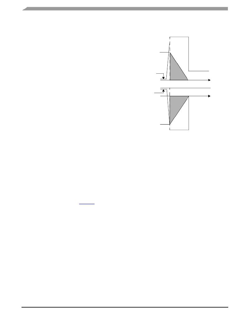
�OUTPUT� VOLTAGE� CLAMP�
�Each� output� of� the� 33880� incorporates� an� internal� voltage�
�clamp� to� provide� fast� turn-off� and� transient� protection� of� each�
�output.� Each� clamp� independently� limits� the� drain-to-source�
�voltage� to� 45� V� for� low-side� drive� configurations� and� -20� V� for�
�high-side� drive� configurations� (see� Figure� 25� ).� The� total�
�energy� clamped� (E� J� )� can� be� calculated� by� multiplying� the�
�current� area� under� the� current� curve� (I� A� )� times� the� clamp�
�voltage� (V� CL� ).�
�Characterization� of� the� output� clamps,� using� a� single� pulse�
�non-repetitive� method� at� 0.3� A,� indicates� the� maximum�
�Figure� 25.� Output� Voltage� Clamping�
�SPI� CONFIGURATIONS�
�The� SPI� configuration� on� the� 33880� device� is� consistent�
�with� other� devices� in� the� OSS� family.� This� device� may� be�
�used� in� serial� SPI� or� parallel� SPI� with� the� 33291� and� 33298.�
�Different� SPI� configurations� may� be� provided.� For� more�
�information,� contact� Analog� Products� Division.�
�REVERSE� BATTERY�
�The� 33880� has� been� designed� with� reverse� battery�
�protection� on� the� VPWR� pin.� However,� the� device� does� not�
�protect� the� load� from� reverse� battery.� During� the� reverse�
�battery� condition,� current� will� flow� through� the� load� via� the�
�output� MOSFET� substrate� diode.� Under� this� circumstance�
�relays� may� energize� and� lamps� will� turn� on.� If� load� reverse�
�battery� protection� is� desired,� a� diode� must� be� placed� in� series�
�with� the� load.�
�energy� to� be� 50� mJ� at� 150� °� C� junction� temperature� per� output.�
�33880�
�Analog� Integrated� Circuit� Device� Data�
�18�
�Freescale� Semiconductor�
�发布紧急采购,3分钟左右您将得到回复。
相关PDF资料
KIT33886DHEVB
KIT EVAL FOR MC33886 H-BRIDGE
KIT33887EKEVBE
BOARD EVALUATION FOR MC33887
KIT33887PNBEVB
KIT EVAL 33887 5A H-BRIDGE PQFN
KIT33905D5EKEVBE
KIT EVALUATION FOR MC33905
KIT33912EVME
KIT EVALUATION FOR MC33912
KIT33932VWEVBE
KIT EVALUATION FOR MC33932
KIT33982CEVBE
KIT EVAL 33982 HIGH SIDE SWITCH
KIT33984CEVBE
KIT EVAL 33984 HIGH SIDE SWITCH
相关代理商/技术参数
KIT33883DWEVB
功能描述:KIT EVAL FOR MC33883 PRE-DRIVER RoHS:否 类别:编程器,开发系统 >> 过时/停产零件编号 系列:- 标准包装:1 系列:- 传感器类型:CMOS 成像,彩色(RGB) 传感范围:WVGA 接口:I²C 灵敏度:60 fps 电源电压:5.7 V ~ 6.3 V 嵌入式:否 已供物品:成像器板 已用 IC / 零件:KAC-00401 相关产品:4H2099-ND - SENSOR IMAGE WVGA COLOR 48-PQFP4H2094-ND - SENSOR IMAGE WVGA MONO 48-PQFP
KIT33886DHEVB
功能描述:电源管理IC开发工具 33886 PWR H-BRIDGE KIT RoHS:否 制造商:Maxim Integrated 产品:Evaluation Kits 类型:Battery Management 工具用于评估:MAX17710GB 输入电压: 输出电压:1.8 V
KIT33887DWBEVB
功能描述:电源管理IC开发工具 33887DWB FIESTA EVAL KIT RoHS:否 制造商:Maxim Integrated 产品:Evaluation Kits 类型:Battery Management 工具用于评估:MAX17710GB 输入电压: 输出电压:1.8 V
KIT33887EKEVBE
功能描述:电源管理IC开发工具 33887DWB FIESTA EVAL KIT RoHS:否 制造商:Maxim Integrated 产品:Evaluation Kits 类型:Battery Management 工具用于评估:MAX17710GB 输入电压: 输出电压:1.8 V
KIT33887EKEVBE
制造商:Freescale Semiconductor 功能描述:5.2A 20KHz Inductive load driver w/ Curr
KIT33887PNBEVB
功能描述:电源管理IC开发工具 33887 FIESTA PNB KIT RoHS:否 制造商:Maxim Integrated 产品:Evaluation Kits 类型:Battery Management 工具用于评估:MAX17710GB 输入电压: 输出电压:1.8 V
KIT33903BD3EVBE
功能描述:界面开发工具 3V DUAL LIN EVB KIT RoHS:否 制造商:Bourns 产品:Evaluation Boards 类型:RS-485 工具用于评估:ADM3485E 接口类型:RS-485 工作电源电压:3.3 V
KIT33903BD5EVBE
功能描述:界面开发工具 5V DUAL LIN EVB KIT
RoHS:否 制造商:Bourns 产品:Evaluation Boards 类型:RS-485 工具用于评估:ADM3485E 接口类型:RS-485 工作电源电压:3.3 V